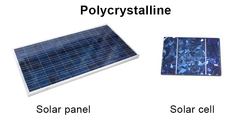

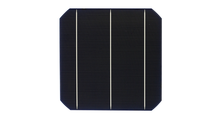
Polycrystalline
Overview and Appearance
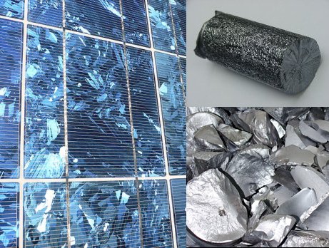
Polycrystalline or Multicrystalline are a newer technology and vary in the manufacturing process.
Construction
Polycrystalline also start as a silicon crystal ‘seed’ placed in a vat of molten silicon. However, rather than draw the silicon crystal seed up as with Monocrystalline the vat of silicon is simply allowed to cool. This is what forms the distinctive edges and grains in the solar cell.
Polycrystalline cells were previously thought to be inferior to Monocrystalline because they were slightly less efficient, however, because of the cheaper method by which they can be produced coupled with only slightly lower efficiencies they have become the dominant technology on the residential solar panels market.
In November 2015 Trina Solar announced that it had produced a multi-crystalline cell with efficiency of 21.25%. This should allow them to produce polycrystalline modules with efficiencies between 18-20% a concept that was thought impossible as recently as 2013.
Underpinning the new record for p-type multicrystalline solar cells has been the continued quality improvements of multicrystalline wafers that have helped pushed standard 60-cell multicrystalline panels from 240W to 260W in recent years.
Polycrystalline are now very close to Monocrystalline cells in terms of efficiency.
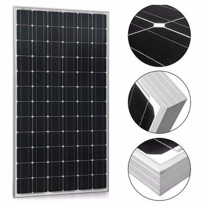
Monocrystalline
Overview and Appearance
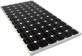
This is the oldest and most developed of the three technologies. Monocrystalline panels as the name suggests are created from a single continuous crystal structure. A Monocrystalline panel can be identified from the solar cells which all appear as a single flat color.
Construction
They are made through the Czochralski method where a silicon crystal ‘seed’ is placed in a vat of molten silicon. The seed is then slowly drawn up with the molten silicon forming a solid crystal structure around the seed known as an ingot. The ingot of solid crystal silicon that is formed is then finely sliced ingot what is known as a silicon wafer. This is then made into a cell.
The Czochralski process results in large cylindrical ingots. Four sides are cut out of the ingots to make silicon wafers. A significant amount of the original silicon ends up as waste.

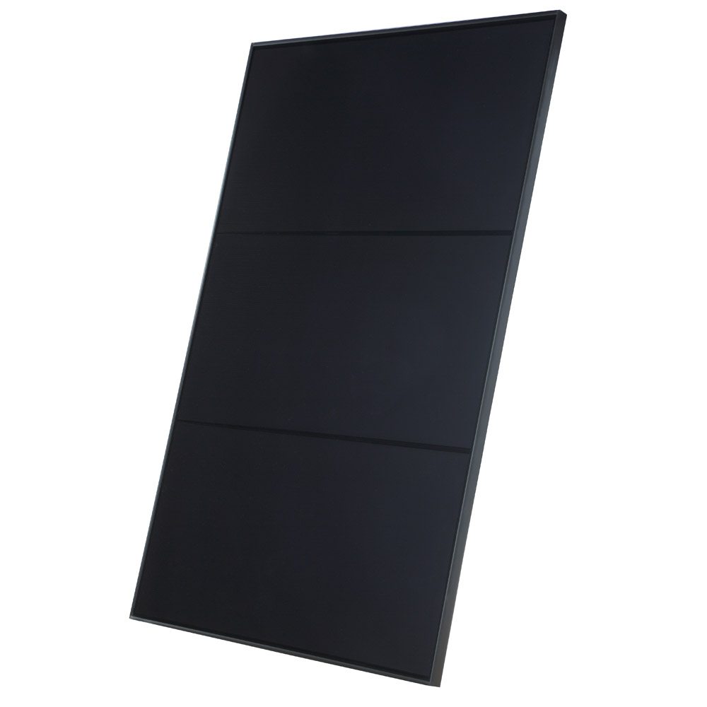
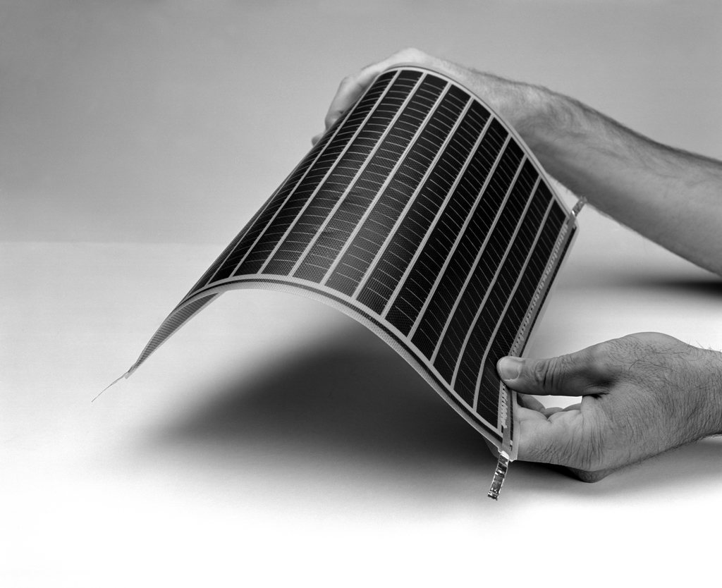
Thin Film
Overview and Appearance
Thin film panels are a totally different technology to Mono and Polycrystalline panels. They are a new technology compared to Mono and Polycrystalline cells and would not be considered a mature technology as vast improvements in this technology are expected in the next 10 years.
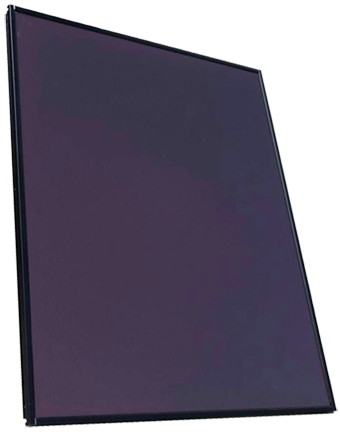
A thin film panel can be identified as having a solid black appearance. They may or may not have a frame, if the panel has no frame it is a thin film panel.
Construction
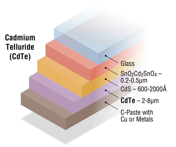
Thin film panels are made by depositing a photovoltaic substance onto a solid surface like glass. The photovoltaic substance that is used varies and multiple combinations of substances have successfully and commercially been used. Examples of the most common photovoltaic substances used are:
- Amorphous Silicon
- Cadmium Telluride (CdTe)
- Copper indium gallium selenide (CGIS)
- Dye-sensitized solar cell (DSC)
Each of the above are known as different panel 'types' but all fall under the umbrella of being a Thin Film panel.
Performance
Thin film cells have got a reputation as being the ‘worst’ of the solar panel technologies because they have the lowest efficiency. However, this is only because they have a lower power efficiency which only means they require the most space for the same amount of power. Since they are becoming the cheapest panels to produce because of the low material costs for thin film they are quickly becoming the more economically efficient panel types.
Depending on the technology, thin-film module prototypes have reached efficiencies between 7–13% and production modules operate at about 9%. Future module efficiencies are expected to climb close to the about 10–16%.
The market for thin-film PV grew at a 60% annual rate from 2002 to 2007. In 2011, close to 5% of U.S. photovoltaic module shipments to the residential sector were based on thin-film